


Dr. Eduardo Martínez Guerra
Researcher
Phone: +52 (81) 1156 0813
Email: eduardo.martinez@cimav.edu.mx
Academic Biography
- 1999-2004, PhD, Material Science, Center of Scientific Research and Post-grade Education of Ensenada (CICESE), B.C., MEXICO.
- 1997-1999, Master of Science, Material Science, Center of Scientific Research and Post-grade Education of Ensenada (CICESE), B.C., MEXICO.
- 1993-1997, Bachelor of Science, Physics, Autonomous National University of Nuevo León, MEXICO.
- Post Doctoral Research Associate, Department of Materials Science and Engineering, Centro de Ciencias de la Materia Condensada, Universidad Nacional Autónoma de México, Ensenada, B.C. 22800.
- August 1998-January 2005, Profesor in University of Baja California, MEXICO.
- August 1999-December 2004 Member of Technical Staff in Department of Materials Science and Engineering, CCMC-UNAM, B.C.,MEXICO.
- August 2002- January 2005, Profesor in the Technologic Institute of Ensenada, B.C., MEXICO.
Research
Nanomaterials by Atomic layer deposition (ALD): This is a thin film growth technique that uses alternating, self-limiting chemical reactions to deposit materials in an atomic layer-by-layer fashion. Although this process is already used commercially for microelectronics manufacturing, ALD promises to have a much broader impact extending far beyond microelectronics. In particular, the capability to infiltrate and coat nanoporous substrates coupled with a broad palate of available materials make ALD a versatile technique for synthesizing nanostructured materials. We are pursuing a variety of new applications for ALD including photovoltaics, catalysis, and energy storage. A central theme in these efforts is that we use ALD to apply precise, conformal coatings onto nanostructured scaffolds to impart the desired optical, electrical, or chemical properties to advance these technologies.

Figure 2. Diagram that describes our research interests.
Some specifics topics of our interests are: Thin Film growth and materials physics of complex oxides: Structure-Property Processing interrelationships; Crystalline Oxide on Semiconductors; Functional metal oxide thin film deposition and processing for microelectronic, magneto-electronic, and optical and high frequency applications, Electrical Degradation processes in ferroelectric systems. Oxide Thin Film Heterostructures: Growth mechanisms and defect structures; Multiferroic oxide heterostructures; transport phenomena in highly correlated systems.
Figure 3. a) Relation between synthesis, properties, structure and composition with modeling, b) Ferroelectric Heterostructure c) Plasma generated for Ion Sputtering for growing ferroelectric thin films.
Nanoparticles: The group focuses on concepts, properties, phenomena, and processes related to nanoparticles, tubes, layers, clusters and other finite structures of the nanoscale size range. Coverage includes synthesis, assembly, transport, reactivity, and stability, and emphasizes realization and application of systems, structures and devices with novel functions obtained via precursor nanoparticles.
Some specifics topics of our interests are: Shyntesis and characterization of Multiferroic Nanostructures and Physical Properties of quantum dots.
Figure 1. Laboratory for Atomic Layer Deposition and Semiconductor oxides grown by ALD for nanodevices.
Electroceramics: The Electroceramics Research Group at CIMAV has been conducting research mainly on the development of composite piezoelectric sensors and actuators, piezoelectric thin films for electromechnical applications, multilayer capacitors, and size effects in nano-ferroelectric systems.
Thin Films: our aim is to increase the fundamental understanding of vapor phase growth and reactions in thin films on an atomistic level, and to explore physical properties of structures unique to thin solid films. The strategy is to carry out basic research studies for describing the relationships between growth parameters, structure/composition and physical properties of thin films. The research covers several materials and growth techniques, and often forms the basis for new materials and processes of interest for future applications.
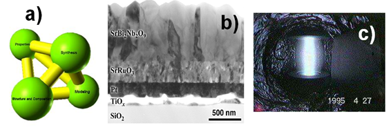
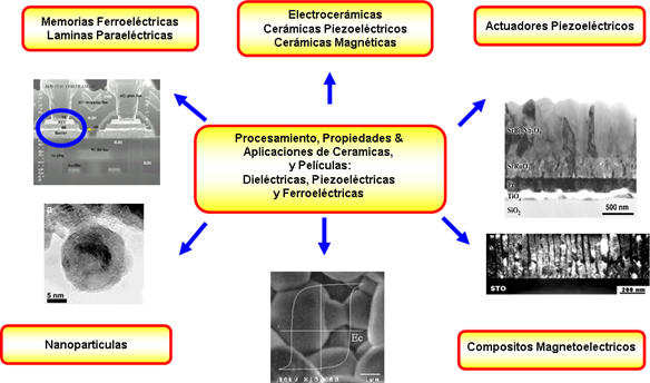
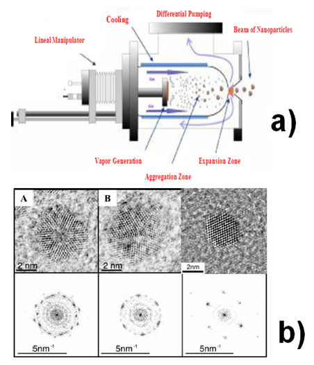
Figure 4 a) Representation for Synthesis of nanoparticles obtained by Inert Gas Condensation Technique b) Micrographs of nanoparticles analyzed by HRTEM.
Research Experience
Epitaxial growth of oxide thin films on semiconductors using Ion- Sputtering Technique.
Structural Characterization of functional ferroelectric thin films using four circle X-Ray Diffraction and morphological characterization using Atomic Force Microscopy.
Electrical Characterization of ferroelectric ceramics and thin films.
Knowledge of vacuum technology and equipments.
Selected Publications (5)
- "Dielectric and Phase Transition Properties of Gd Doped PbZr0.53Ti0.47O3" J. Portelles, N.S. Almodóvar, E.Martínez, O.Raymond, J.Heiras, and J. M. Siqueiros. Integrated Ferroelectrics, 2009, 101, 70.
- "Synthesis and Dielectric Properties of (Pb,La)(Zr,Ti)O3 Ferroelectric Ceramics" O.Blanco, E.Martínez, J.Vital, A. Correa. Integrated Ferroelectrics, 2009, 101, 44.
- "Ferroelectric hysteresis and aging effect analysis in multiferroic PbFe0.5Nb0.5O3 ceramics" R. Font, O. Raymond, E. Martinez, J. Portelles and J. M. Siqueiros. Journal of Applied Physics, 2009, 105, 114110.
- "Temperature dependent thermal conductivity of polycrystalline ZnO films" J. Alvarez-Quintana, E. Martínez, E. Pérez-Tijerina, S. A. Pérez-García, and J. Rodríguez-Viejo. Journal of Applied Physics, 2010, 107, 63713.
- "ZnO nanowires: Growth of ZnO Nanowires Using Au/Pd Nanoparticles as Catalyst" Francisco Solís-Pomar, Eduardo Martínez-Guerra, Manuel Meléndrez-Castro and Eduardo Pérez-Tijerina. Journal of Nanoresearch, 2011, 14, 147.